In the ever-evolving landscape of materials science and analysis, energy-dispersive X-ray spectroscopy (EDS or EDX) stands out as a critical tool for researchers, engineers, and quality control professionals. When paired with scanning electron microscopy (SEM), EDS transforms a high-resolution image into a rich map of elemental composition—unlocking the secrets hidden within the microstructure of materials.
From quality control and failure analysis in manufacturing to advanced research in academic laboratories, SEM-EDS empowers users to not only visualize but also understand the elemental composition of materials at the micro and nanoscale.
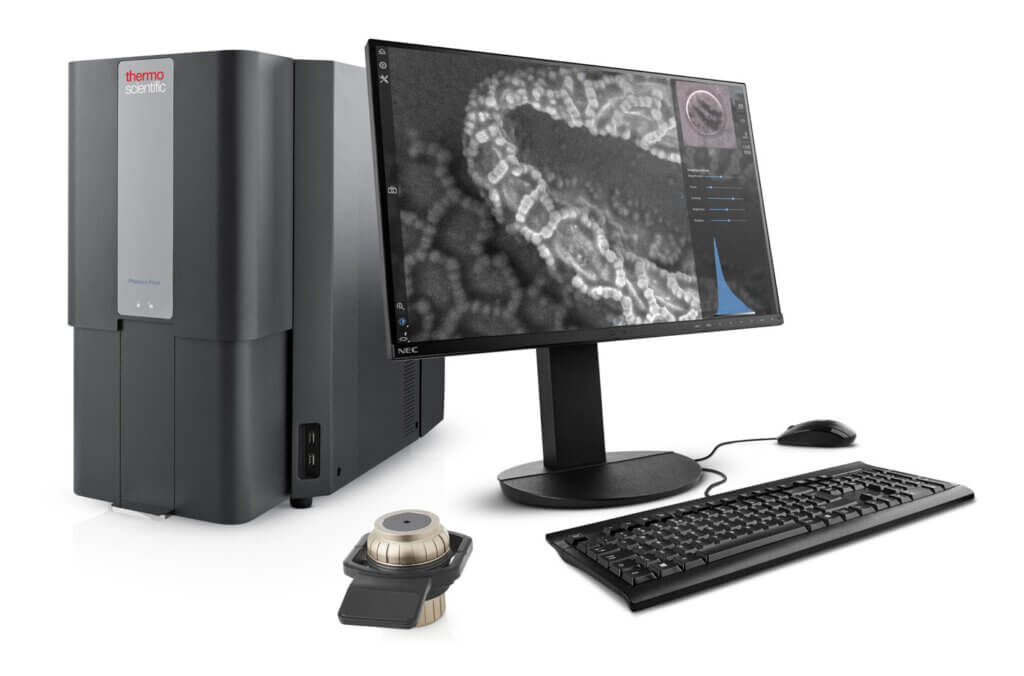
At the forefront of this innovation is the Thermo Scientific Phenom desktop SEM, a compact and intuitive SEM platform that brings powerful EDX capabilities into everyday laboratories and production environments. The Phenom desktop SEM systems combine high-performance imaging with powerful, user-friendly EDX capabilities. With features such as live elemental mapping, automated drift correction, and intuitive data processing, the Phenom desktop SEMs provide a seamless and efficient workflow.
What is EDS and how does it work
Energy-dispersive X-ray spectroscopy is a non-destructive technique that identifies and quantifies the elements within a sample by detecting the characteristic X-rays emitted when the sample is hit by a focused electron beam. Each element emits X-rays at unique energy levels, allowing the EDS detector to provide both qualitative and quantitative data on the sample’s composition. When used in conjunction with SEM imaging, this enables simultaneous morphological and elemental analysis of the same region of interest.

To learn more about the principles and applications of EDS in compact SEM systems, check out this article on chemical analysis using desktop SEM microscopes.
Versatility and wide range of applications
One of EDS’s greatest strengths is its adaptability. It can be used across a broad range of materials—from metals and ceramics to polymers and biological specimens. EDS identifies major, minor, and trace elements, making it invaluable for detecting defects, contaminants, or inclusions at the micro and nanoscale. And since the technique is non-destructive, the sample remains intact for further testing or archiving.
In industrial settings, EDS plays a vital role in quality assurance. It helps verify material composition, pinpoint impurities, and trace the origin of defects—contributing to better process control and product consistency. High-throughput systems like the Phenom XL SEM support large-area analysis, making them ideal for production environments.
In regulated industries like pharmaceuticals and food, EDS ensures compliance and batch uniformity. In academic and R&D labs, it’s essential for in-depth material characterization. Researchers working at higher resolutions can benefit from tools like the Phenom Pharos, which offers field emission imaging and EDS integration.
Want to read the full article?
Read the full article on our specialised website: electron-microscopes.com.